



 本文介绍了数字时钟的设计过程,包括使用EDA中的数码管动态显示时分秒的电路模型、参考程序以及实验仿真。详细解析了计数器驱动数码管显示的方法,并展示了时钟电路模块的实现和实验效果。
提示:文章写完后,目录可以自动生成,如何生成可参考右边的帮助文档
文章目录
前言
提示:这里可以添加本文要记录的大概内容:
前面学习了基本的数字芯片逻辑编程,学会了计数器等,这次来一个做一个综合应用。数字时钟,采用数码管显示时分秒。
提示:以下是本篇文章正文内容,下面案例可供参考
一、数字时钟是什么?
数字时钟是一种以数字显示取代模拟表盘的钟表,它能够以数字的形式显示当前的时间,并且可以同时显示时、分、秒。此外,它通常具有对时、分、秒进行准确校准的功能。
示例:能用数码管显示 时分秒的时钟
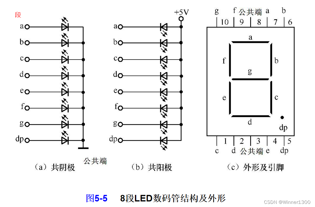
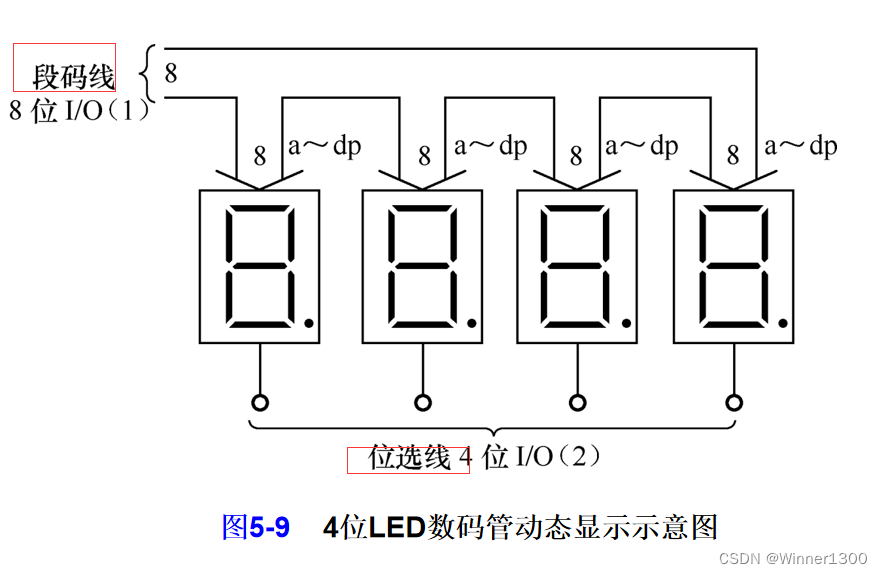
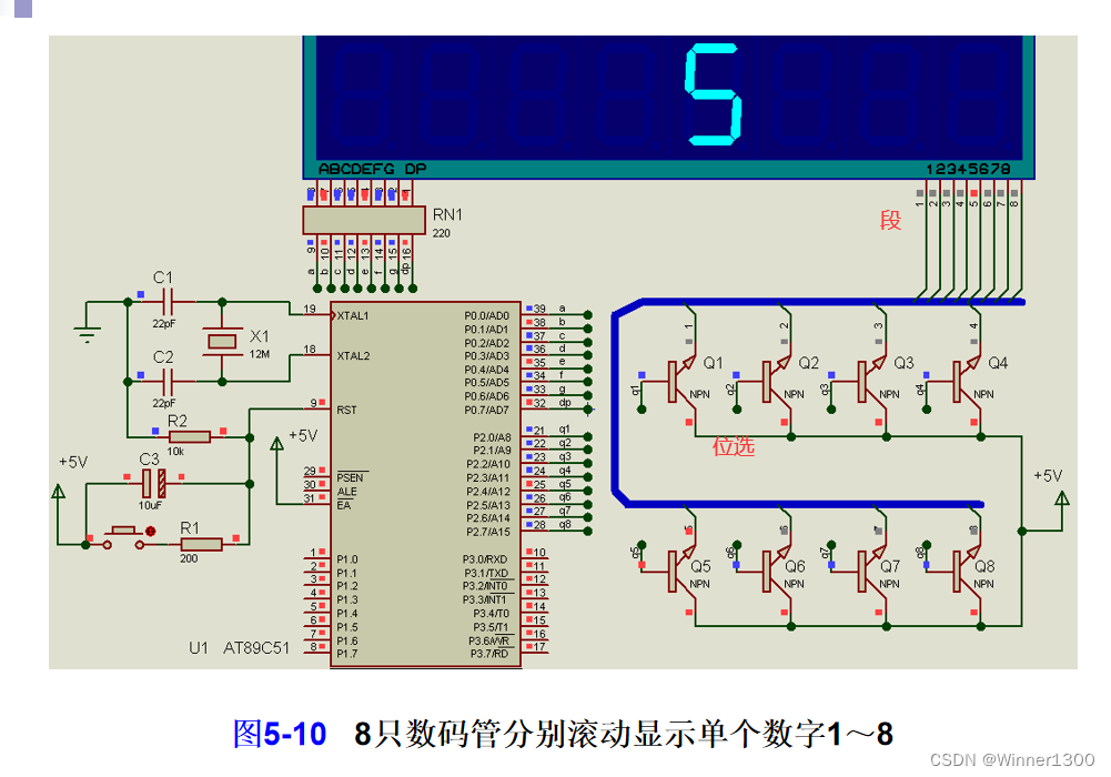
二、EDA里面数码管的显示
目标:动态数码管显示: 12345678
时间显示的状态效:”12.20.30 12-20.30 12-20-30
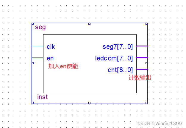
1.元件模型
代码如下(示例):
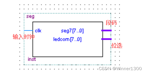
2.参考程序
代码如下(示例):
module seg(clk,seg7,ledcom);
input clk; // 假设系统提供的时钟 50Mhz
output[7:0] seg7; //段
output[7:0] ledcom; //位选
reg[7:0] seg7;  //alway 里面赋值要用reg数据
reg[20:0] cnt;
reg[7:0] ledcom;
always@(posedge clk)
begin
 if(cnt==21'b1 1111 1111 1111 1111 1111) // 2的22减一
 cnt<=0;
 else
 cnt<=cnt+1;
end
always@(cnt) //给位选
begin
 case(cnt[16:14])    // 14  15  16   000 ->111   前面13为 满进位
 3'b000:ledcom<=8'b00000001;//0   只有一个位选为1 只有第一位数码管选中并显示
 3'b001:ledcom<=8'b00000010;//1
 3'b010:ledcom<=8'b00000100;//2
 3'b011:ledcom<=8'b00001000;//3
 3'b100:ledcom<=8'b00010000;//0
 3'b101:ledcom<=8'b00100000;//1
 3'b110:ledcom<=8'b01000000;//2
 3'b111:ledcom<=8'b10000000;//3
 endcase
end
always@(cnt) //段码
begin
 case(cnt[16:14])
 3'b000:seg7<=8'b00000111;//0  同时给到段码 ,保证只有 第一个数码管亮
 3'b001:seg7<=8'b11011011;//1
 3'b010:seg7<=8'b11001111;//2
  3'b011:seg7<=8'b10100111;//3
 3'b100:seg7<=8'b11101101;//0
 3'b101:seg7<=8'b11111101;//1
 3'b110:seg7<=8'b01000111;//2
 3'b111:seg7<=8'b11111111;//3
 endcase
end
endmodule
为了仿真改小了参数
module seg(clk,seg7,ledcom,cnt,en);
input en;
input clk; // 假设系统提供的时钟 50Mhz
output[7:0] seg7; //段
output[7:0] ledcom; //位选
reg[7:0] seg7;  //alway 里面赋值要用reg数据
output reg[8:0] cnt;
reg[7:0] ledcom;
always@(posedge clk)
begin
	if(!en)
	cnt<=0;
	else
		if(cnt==8'b111111111) // 2的22减一
		cnt<=0;
		else
		cnt<=cnt+1;
end
always@(cnt) //给位选
begin
 case(cnt[7:5])    // 14  15  16   000 ->111   前面13为 满进位
 3'b000:ledcom<=8'b00000001;//0   只有一个位选为1 只有第一位数码管选中并显示
 3'b001:ledcom<=8'b00000010;//1
 3'b010:ledcom<=8'b00000100;//2
 3'b011:ledcom<=8'b00001000;//3
 3'b100:ledcom<=8'b00010000;//0
 3'b101:ledcom<=8'b00100000;//1
 3'b110:ledcom<=8'b01000000;//2
 3'b111:ledcom<=8'b10000000;//3
  default:ledcom<=8'b10000000;
 endcase
end
always@(cnt) //段码
begin
 case(cnt[7:5])
 3'b000:seg7<=8'b00000111;//0  同时给到段码 ,保证只有 第一个数码管亮
 3'b001:seg7<=8'b11011011;//1
 3'b010:seg7<=8'b11001111;//2
  3'b011:seg7<=8'b10100111;//3
 3'b100:seg7<=8'b11101101;//0
 3'b101:seg7<=8'b11111101;//1
 3'b110:seg7<=8'b01000111;//2
 3'b111:seg7<=8'b11111111;//3
 default:seg7<=8'b11111111;
 endcase
end
endmodule
测试文件
`timescale 1 ps/ 1 ps
module seg_tb3();
// constants
// general purpose registers
reg eachvec;
// test vector input registers
reg clk;
reg en;
// wires
wire [8:0]  cnt;
wire [7:0]  ledcom;
wire [7:0]  seg7;

// assign statements (if any)
seg i1 (
// port map - connection between master ports and signals/registers
	.clk(clk),
	.cnt(cnt),
	.en(en),
	.ledcom(ledcom),
	.seg7(seg7)
);
initial
begin
// code that executes only once
// insert code here --> begin

// --> end
#10 clk= 0;
#100 en=0;
#10 en=1;
$display("Running testbench");
end

always #10 clk=~clk;
always
// optional sensitivity list
// @(event1 or event2 or .... eventn)
begin
// code executes for every event on sensitivity list
// insert code here --> begin

@eachvec;
// --> end
end
endmodule
实际仿真测试元件图
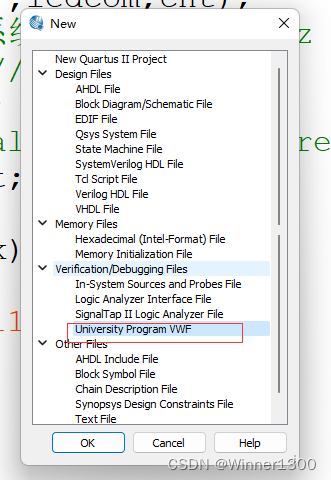
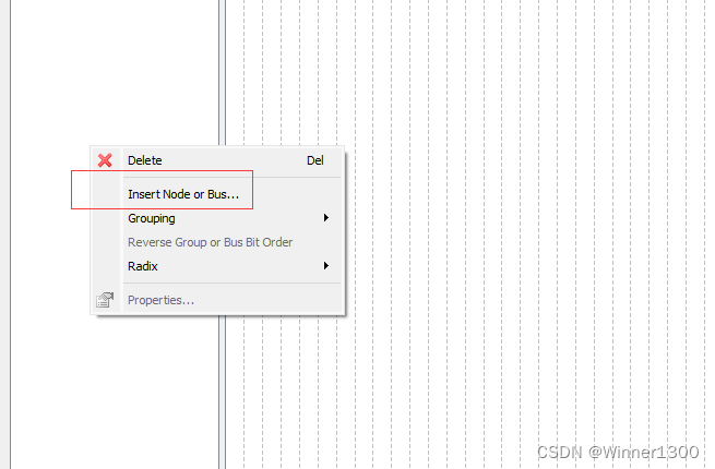
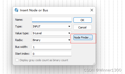
3. 实验仿真波形
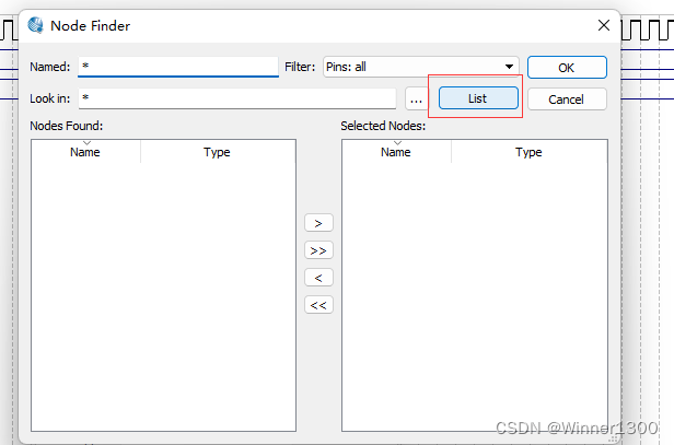
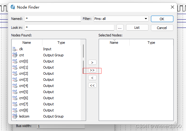
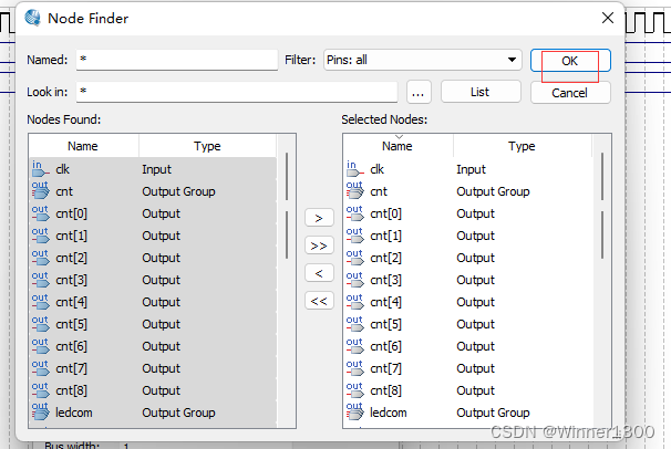
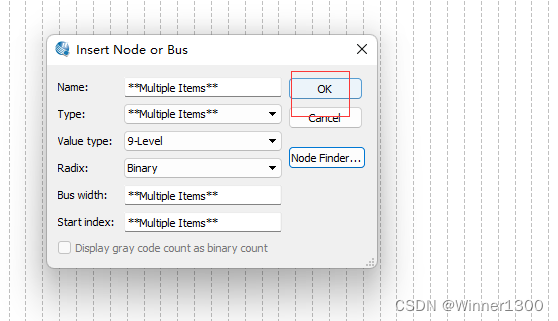
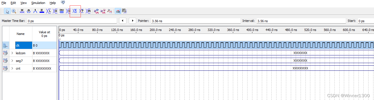
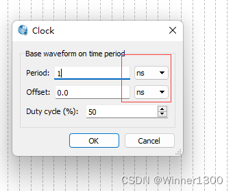
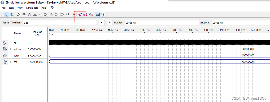
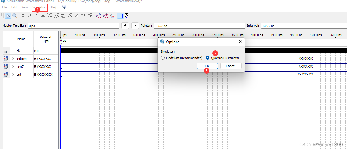
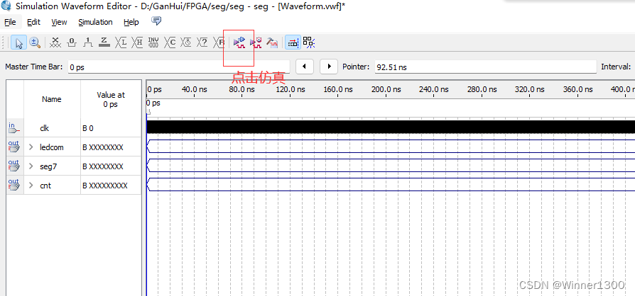

4.实验现象
5. 仿真问题
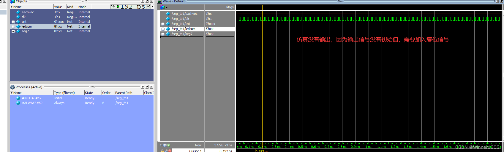
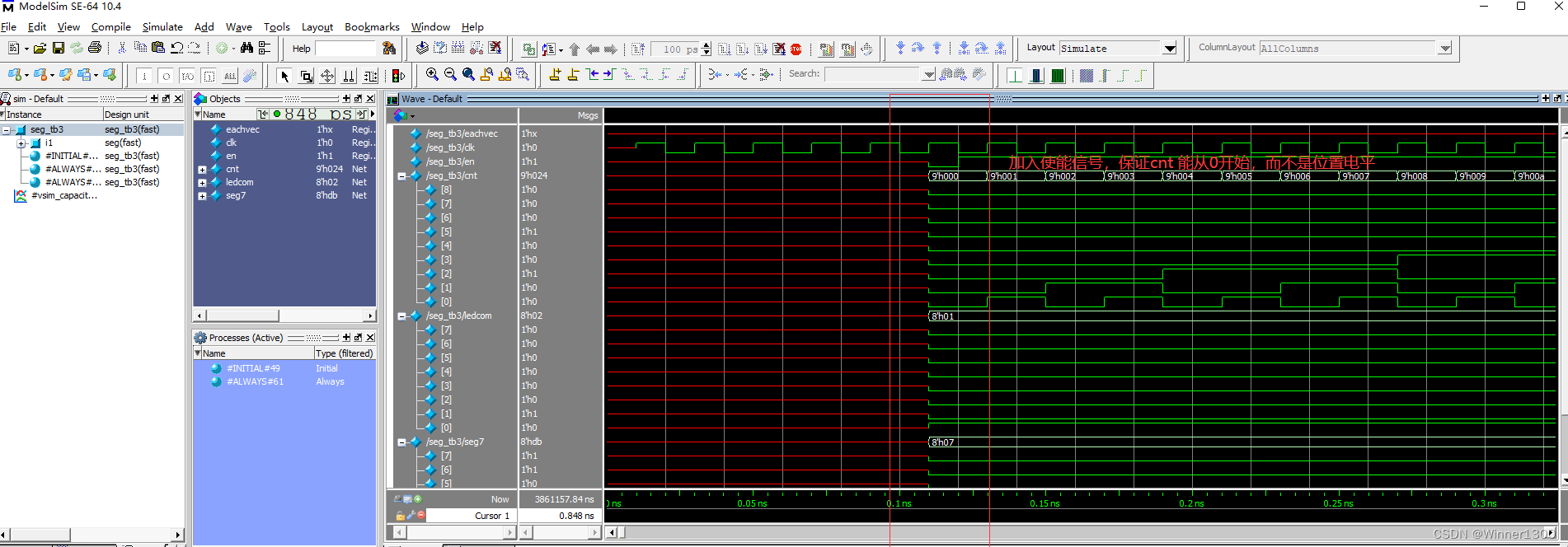
三、显示时钟
1. 时钟电路模块
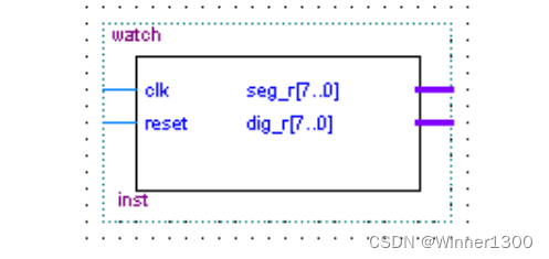
2.参考程序
module watch(clk,reset,seg_r,dig_r);
input clk;
input reset;
output[7:0] seg_r;
output[7:0] dig_r;
reg[25:0] count;
reg[15:0] hour;
reg sec;
reg[4:0] disp_dat;
reg[7:0] seg_r;
reg[7:0] dig_r;
always @(posedge clk)
begin
 count = count + 1'b1;
 if(count == 26'd25000000)
 begin
 count = 26'd0;
 sec = ~sec;
 end
end
always @(posedge sec)
begin
if(reset==0)
 hour[15:0]=0;
 else
 begin
 hour[3:0] = hour[3:0]+1'b1;
 if(hour[3:0] == 4'ha)
 begin
 hour[3:0] = 4'h0;
 hour[7:4] = hour[7:4]+1'b1;
 if(hour[7:4] == 4'h6)
 begin
 hour[7:4] = 4'h0;
 hour[11:8] = hour[11:8] + 1'b1;
 if(hour[11:8] ==4'ha)
 begin
 hour[11:8] = 4'h0;
 hour[15:12] = hour[15:12] + 1'b1;
 if(hour[15:12] == 4'h6)
 hour[15:12] =4'h0;
 end
 end
 end
 end
 end
always @(posedge clk)
begin
 case(count[17:15])
 3'd0:disp_dat = hour[3:0];
 3'd1:disp_dat = hour[7:4];
 3'd3:disp_dat = hour[11:8];
 3'd4:disp_dat = hour[15:12];
 endcase
 case(count[17:15])
 3'd0:dig_r = 8'b10000000;
 3'd1:dig_r = 8'b01000000;
 3'd2:dig_r = 8'b00000000;
 3'd3:dig_r = 8'b00010000;
 3'd4:dig_r = 8'b00001000;
 3'd5:dig_r = 8'b00000000;
 3'd6:dig_r = 8'b00000000;
 3'd7:dig_r = 8'b00000000;
 endcase
end
always @(posedge clk)
begin
 case(disp_dat)
0:seg_r=8'b01111111;
 1:seg_r=8'b00000111;
 2:seg_r=8'b11011011;
 3:seg_r=8'b11001111;
 4:seg_r=8'b10100111;
 5:seg_r=8'b11101101;
 6:seg_r=8'b11111101;
 7:seg_r=8'b01000111;
 8:seg_r=8'b11111111;
 9:seg_r=8'b11101111;
default:seg_r = 8'hff;
 endcase
end
endmodule
3.tcl引脚配置
# Setup pin setting for EP2C8 main board
set_global_assignment -name RESERVE_ALL_UNUSED_PINS "AS INPUT TRI-STATED"
set_global_assignment -name ENABLE_INIT_DONE_OUTPUT OFF
#clk
set_location_assignment PIN_P1 -to clk

#beep
set_location_assignment PIN_T18 -to beep
#led
set_location_assignment PIN_H23 -to led\[0\]
set_location_assignment PIN_G26 -to led\[1\]
set_location_assignment PIN_G25 -to led\[2\]
set_location_assignment PIN_K22 -to led\[3\]
set_location_assignment PIN_G24 -to led\[4\]
set_location_assignment PIN_G23 -to led\[5\]
set_location_assignment PIN_P18 -to led\[6\]
set_location_assignment PIN_N18 -to led\[7\]

#rst
set_location_assignment PIN_R4 -to reset
#key
set_location_assignment PIN_F26 -to key\[0\]
set_location_assignment PIN_F25 -to key\[1\]
set_location_assignment PIN_J20 -to key\[2\]
set_location_assignment PIN_J21 -to key\[3\]
set_location_assignment PIN_F23 -to key\[4\]
set_location_assignment PIN_F24 -to key\[5\]
set_location_assignment PIN_E25 -to key\[6\]
set_location_assignment PIN_E26 -to key\[7\]
#seg7led
set_location_assignment PIN_K19 -to ledcom\[0\]
set_location_assignment PIN_K18 -to ledcom\[1\]
set_location_assignment PIN_H19 -to ledcom\[2\]
set_location_assignment PIN_H26 -to ledcom\[3\]
set_location_assignment PIN_H25 -to ledcom\[4\]
set_location_assignment PIN_J24 -to ledcom\[5\]
set_location_assignment PIN_J23 -to ledcom\[6\]
set_location_assignment PIN_H24 -to ledcom\[7\]

set_location_assignment PIN_K21 -to seg7\[0\]
set_location_assignment PIN_J26 -to seg7\[1\]
set_location_assignment PIN_J25 -to seg7\[2\]
set_location_assignment PIN_L20 -to seg7\[3\]
set_location_assignment PIN_L21 -to seg7\[4\]
set_location_assignment PIN_K24 -to seg7\[5\]
set_location_assignment PIN_L23 -to seg7\[6\]
set_location_assignment PIN_K23 -to seg7\[7\]

#PS2
set_location_assignment PIN_U23 -to data
set_location_assignment PIN_P24 -to kbclk

#lcd128*64
set_location_assignment PIN_R19 -to rs1
set_location_assignment PIN_U21 -to rs2
set_location_assignment PIN_U20 -to rs
set_location_assignment PIN_T19 -to en
set_location_assignment PIN_U24 -to rw
set_location_assignment PIN_V26 -to dat\[0\]
set_location_assignment PIN_V25 -to dat\[1\]
set_location_assignment PIN_V24 -to dat\[2\]
set_location_assignment PIN_V23 -to dat\[3\]
set_location_assignment PIN_W26 -to dat\[4\]
set_location_assignment PIN_W25 -to dat\[5\]
set_location_assignment PIN_W23 -to dat\[6\]
set_location_assignment PIN_W24 -to dat\[7\]


#rxd
set_location_assignment PIN_H24 -to rxd
set_location_assignment PIN_H26 -to txd

set_location_assignment PIN_T23 -to rxd_usb
set_location_assignment PIN_P17 -to txd_usb

#VGA
set_location_assignment PIN_R25 -to hs
set_location_assignment PIN_T22 -to vs
set_location_assignment PIN_V25 -to red
set_location_assignment PIN_V24 -to grn
set_location_assignment PIN_T24 -to blu

#inter
set_location_assignment PIN_AE4  -to   inter1_1[0]
set_location_assignment PIN_AC6  -to   inter1_1[1]
set_location_assignment PIN_AE5  -to   inter1_1[2]
set_location_assignment PIN_AD7  -to   inter1_1[3]
set_location_assignment PIN_AC7  -to   inter1_1[4]
set_location_assignment PIN_Y10  -to   inter1_1[5]
set_location_assignment PIN_AD8  -to   inter1_1[6]
set_location_assignment PIN_AA10 -to   inter1_1[7]
set_location_assignment PIN_AE7  -to   inter1_1[8]
set_location_assignment PIN_AF8  -to   inter1_1[9]
set_location_assignment PIN_AC9  -to   inter1_1[10]
set_location_assignment PIN_AF9  -to   inter1_1[11]
set_location_assignment PIN_AE10 -to   inter1_1[12]
set_location_assignment PIN_AE12 -to   inter1_1[13]
set_location_assignment PIN_AE11 -to   inter1_1[14]
set_location_assignment PIN_Y12  -to   inter1_1[15]
set_location_assignment PIN_V13  -to   inter1_1[16]
set_location_assignment PIN_AC12 -to   inter1_1[17]
set_location_assignment PIN_W17  -to   inter1_1[18]
set_location_assignment PIN_AE19 -to   inter1_1[19]
set_location_assignment PIN_AF18 -to   inter1_1[20]
set_location_assignment PIN_AD17 -to   inter1_1[21]
set_location_assignment PIN_AF17 -to   inter1_1[22]
set_location_assignment PIN_AC16 -to   inter1_1[23]
set_location_assignment PIN_AC15 -to   inter1_1[24]
set_location_assignment PIN_Y15  -to   inter1_1[25]
set_location_assignment PIN_Y13  -to   inter1_1[26]
set_location_assignment PIN_AD15 -to   inter1_1[27]
set_location_assignment PIN_AD19 -to   inter1_1[28]
set_location_assignment PIN_AA18 -to   inter1_1[29]
set_location_assignment PIN_U17  -to   inter1_1[30]
set_location_assignment PIN_AE21 -to   inter1_1[31]
set_location_assignment PIN_AB20 -to   inter1_1[32]
set_location_assignment PIN_V18  -to   inter1_1[33]
set_location_assignment PIN_AF22 -to   inter1_1[34]
set_location_assignment PIN_AD22 -to   inter1_1[35]
set_location_assignment PIN_AE23 -to   inter1_1[36]


set_location_assignment PIN_AF4  -to   inter1_2[0]
set_location_assignment PIN_AD4  -to   inter1_2[1]
set_location_assignment PIN_AF5  -to   inter1_2[2]
set_location_assignment PIN_V10  -to   inter1_2[3]
set_location_assignment PIN_W8   -to   inter1_2[4]
set_location_assignment PIN_AF6  -to   inter1_2[5]
set_location_assignment PIN_AC8  -to   inter1_2[6]
set_location_assignment PIN_AA9  -to   inter1_2[7]
set_location_assignment PIN_AF7  -to   inter1_2[8]
set_location_assignment PIN_W11  -to   inter1_2[9]
set_location_assignment PIN_AC10 -to   inter1_2[10]
set_location_assignment PIN_AD10 -to   inter1_2[11]
set_location_assignment PIN_AF10 -to   inter1_2[12]
set_location_assignment PIN_AE13 -to   inter1_2[13]
set_location_assignment PIN_AA11 -to   inter1_2[14]
set_location_assignment PIN_V11  -to   inter1_2[15]
set_location_assignment PIN_U12  -to   inter1_2[16]
set_location_assignment PIN_AD12 -to   inter1_2[17]
set_location_assignment PIN_AC18 -to   inter1_2[18]
set_location_assignment PIN_AF19 -to   inter1_2[19]
set_location_assignment PIN_Y16  -to   inter1_2[20]
set_location_assignment PIN_AC17 -to   inter1_2[21]
set_location_assignment PIN_W16  -to   inter1_2[22]
set_location_assignment PIN_AD16 -to   inter1_2[23]
set_location_assignment PIN_AB15 -to   inter1_2[24]
set_location_assignment PIN_Y14  -to   inter1_2[25]
set_location_assignment PIN_AA13 -to   inter1_2[26]
set_location_assignment PIN_AE15 -to   inter1_2[27]
set_location_assignment PIN_AC19 -to   inter1_2[28]
#clk input
#set_location_assignment PIN_AE14 -to   inter1_2[29]
set_location_assignment PIN_AA20 -to   inter1_2[30]
set_location_assignment PIN_AF21 -to   inter1_2[31]
set_location_assignment PIN_AE20 -to   inter1_2[32]
set_location_assignment PIN_W19  -to   inter1_2[33]
set_location_assignment PIN_AB21 -to   inter1_2[34]
set_location_assignment PIN_AD23 -to   inter1_2[35]
set_location_assignment PIN_R2   -to   inter1_2[36]

#SDRAM
set_location_assignment PIN_AA6  -to   DRAM_ADDR[11]
set_location_assignment PIN_AA7  -to   DRAM_ADDR[10]
set_location_assignment PIN_AC3  -to   DRAM_ADDR[9]
set_location_assignment PIN_AB4  -to   DRAM_ADDR[8]
set_location_assignment PIN_AB3  -to   DRAM_ADDR[7]
set_location_assignment PIN_AE3  -to   DRAM_ADDR[6]
set_location_assignment PIN_AE2  -to   DRAM_ADDR[5]
set_location_assignment PIN_AD3  -to   DRAM_ADDR[4]
set_location_assignment PIN_AD2  -to   DRAM_ADDR[3]
set_location_assignment PIN_Y5   -to   DRAM_ADDR[2]
set_location_assignment PIN_AA5  -to   DRAM_ADDR[1]
set_location_assignment PIN_AC1  -to   DRAM_ADDR[0]
set_location_assignment PIN_AC2  -to   DRAM_DATA[31]
set_location_assignment PIN_AA3  -to   DRAM_DATA[30]
set_location_assignment PIN_AA4  -to   DRAM_DATA[29]
set_location_assignment PIN_AB1  -to   DRAM_DATA[28]
set_location_assignment PIN_AB2  -to   DRAM_DATA[27]
set_location_assignment PIN_W6   -to   DRAM_DATA[26]
set_location_assignment PIN_V7   -to   DRAM_DATA[25]
set_location_assignment PIN_T8   -to   DRAM_DATA[24]
set_location_assignment PIN_R8   -to   DRAM_DATA[23]
set_location_assignment PIN_Y4   -to   DRAM_DATA[22]
set_location_assignment PIN_Y3   -to   DRAM_DATA[21]
set_location_assignment PIN_AA1  -to   DRAM_DATA[20]
set_location_assignment PIN_AA2  -to   DRAM_DATA[19]
set_location_assignment PIN_V6   -to   DRAM_DATA[18]
set_location_assignment PIN_V5   -to   DRAM_DATA[17]
set_location_assignment PIN_Y1   -to   DRAM_DATA[16]
set_location_assignment PIN_W3   -to   DRAM_DATA[15]
set_location_assignment PIN_W4   -to   DRAM_DATA[14]
set_location_assignment PIN_U5   -to   DRAM_DATA[13]
set_location_assignment PIN_U7   -to   DRAM_DATA[12]
set_location_assignment PIN_U6   -to   DRAM_DATA[11]
set_location_assignment PIN_W1   -to   DRAM_DATA[10]
set_location_assignment PIN_W2   -to   DRAM_DATA[9]
set_location_assignment PIN_V3   -to   DRAM_DATA[8]
set_location_assignment PIN_V4   -to   DRAM_DATA[7]
set_location_assignment PIN_T6   -to   DRAM_DATA[6]
set_location_assignment PIN_T7   -to   DRAM_DATA[5]
set_location_assignment PIN_V2   -to   DRAM_DATA[4]
set_location_assignment PIN_V1   -to   DRAM_DATA[3]
set_location_assignment PIN_U4   -to   DRAM_DATA[2]
set_location_assignment PIN_U3   -to   DRAM_DATA[1]
set_location_assignment PIN_U10  -to   DRAM_DATA[0]
set_location_assignment PIN_R7   -to   DRAM_BA[1]
set_location_assignment PIN_R6   -to   DRAM_BA[0]
set_location_assignment PIN_U9   -to   DRAM_DQM[3]
set_location_assignment PIN_U1   -to   DRAM_DQM[2]
set_location_assignment PIN_U2   -to   DRAM_DQM[1]
set_location_assignment PIN_T4   -to   DRAM_DQM[0]
set_location_assignment PIN_T3   -to   DRAM_CAS
set_location_assignment PIN_T2   -to   DRAM_CKE
set_location_assignment PIN_P7   -to   DRAM_CS
set_location_assignment PIN_T9   -to   DRAM_WE
set_location_assignment	PIN_T10  -to   DRAM_RAS
set_location_assignment PIN_P6   -to   DRAM_CLK

#FLASH
set_location_assignment  PIN_C5  -to   FLASH_ADDR[21]
set_location_assignment  PIN_C6  -to   FLASH_ADDR[20]
set_location_assignment  PIN_A4  -to   FLASH_ADDR[19]
set_location_assignment  PIN_B4  -to   FLASH_ADDR[18]
set_location_assignment  PIN_A5  -to   FLASH_ADDR[17]
set_location_assignment  PIN_B5  -to   FLASH_ADDR[16]
set_location_assignment  PIN_B6  -to   FLASH_ADDR[15]
set_location_assignment  PIN_A6  -to   FLASH_ADDR[14]
set_location_assignment  PIN_C4  -to   FLASH_ADDR[13]
set_location_assignment  PIN_D5  -to   FLASH_ADDR[12]
set_location_assignment  PIN_K9  -to   FLASH_ADDR[11]
set_location_assignment  PIN_J9  -to   FLASH_ADDR[10]
set_location_assignment  PIN_E8  -to   FLASH_ADDR[9]
set_location_assignment  PIN_H8  -to   FLASH_ADDR[8]
set_location_assignment  PIN_H10 -to   FLASH_ADDR[7]
set_location_assignment  PIN_G9  -to   FLASH_ADDR[6]
set_location_assignment  PIN_F9  -to   FLASH_ADDR[5]
set_location_assignment  PIN_D7  -to   FLASH_ADDR[4]
set_location_assignment  PIN_C7  -to   FLASH_ADDR[3]
set_location_assignment  PIN_D6  -to   FLASH_ADDR[2]
set_location_assignment  PIN_B7  -to   FLASH_ADDR[1]
set_location_assignment  PIN_A7  -to   FLASH_ADDR[0]
set_location_assignment  PIN_D8  -to   FLASH_DATA[15]
set_location_assignment  PIN_C8  -to   FLASH_DATA[14]
set_location_assignment  PIN_F10 -to   FLASH_DATA[13]
set_location_assignment  PIN_G10 -to   FLASH_DATA[12]
set_location_assignment  PIN_D9  -to   FLASH_DATA[11]
set_location_assignment  PIN_C9  -to   FLASH_DATA[10]
set_location_assignment  PIN_B8  -to   FLASH_DATA[9]
set_location_assignment  PIN_A8  -to   FLASH_DATA[8]
set_location_assignment  PIN_H11 -to   FLASH_DATA[7]
set_location_assignment  PIN_H12 -to   FLASH_DATA[6]
set_location_assignment  PIN_F11 -to   FLASH_DATA[5]
set_location_assignment  PIN_E10 -to   FLASH_DATA[4]
set_location_assignment  PIN_B9  -to   FLASH_DATA[3]
set_location_assignment  PIN_A9  -to   FLASH_DATA[2]
set_location_assignment  PIN_C10 -to   FLASH_DATA[1]
set_location_assignment  PIN_D10 -to   FLASH_DATA[0]
set_location_assignment  PIN_D11 -to   FLASH_OE
set_location_assignment  PIN_B10 -to   FLASH_CE
set_location_assignment  PIN_A10 -to   FLASH_WE
set_location_assignment  PIN_G11 -to   FLASH_RST


# usb-uart
set_location_assignment  PIN_R2 -to   USB_UART_RX
set_location_assignment  PIN_R3 -to   USB_UART_TX
复制后保存为tcl后缀的文件,保留IO口

4.仿真波形
5.实验效果
总结
提示:这里对文章进行总结:


 扫一扫
扫一扫


 2万+
2万+

 被折叠的 条评论
为什么被折叠?
被折叠的 条评论
为什么被折叠?
 到【灌水乐园】发言


